One Dimensional Nanowires
our experts: Roman Kusterer, Daniel Lengle, Moritz Wehrmeister
One dimensional nanostructures show quantum confinement in two dimensions while their length can be in the range of tens of micrometers. Thus, nanowires feature unique physical properties but can also be integrated in microscopic devices. In our research group, nanowires are synthesized, processed, and investigated by, e.g., electrical measurements, optical spectroscopy and surface-potential measurements.
Synthesis
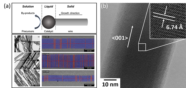
Semiconductor nanowires (NWs) can be prepared in solution by a Solution-Liquid-Solid (SLS) method, in which metal nanoparticles with a low melting point (e.g. bismuth) are used as catalysts (see Fig. 1). The SLS synthesis yields nanowires with diameters between 10 to 30 nm. Besides the SLS method, also solvothermal approaches can be used to obtain high quality (almost monocrystalline) NWs with bigger diameters of around 50 nm (see Fig. 1b). For this reaction, a single-source precursor is dissolved in an organic coordinating solvent and heated up in an autoclave (Ref). This approach allows for very high yields (milligram scale) and a ligand free surface. Our work focuses on the synthesis and characterization of II-VI semiconductor NWs with the composition CdE (E = Se, Te, S) NWs.
Experimental Setup
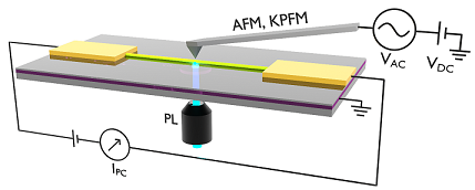
Our setup allows for simultaneous optical, electrical, topographical and surface-potential measurements. For this, single nanowires are deposited (and contacted) on transparent substrates. This enables the excitation of the nanostructure from below while the topography is probed by atomic force microscopy (AFM) from above. Additionally, the surface potential is measured by Kelvin probe force microscopy (KPFM) with or without simultaneous bias potential on the contacted nanowire.
Electrical Measurements
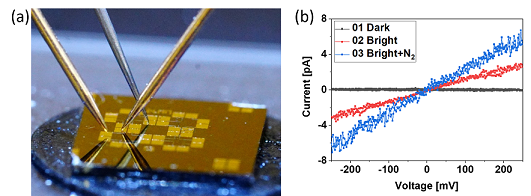
For the electrical characterization of the NWs, field-effect transistors (FETs) are fabricated via optical lithography (see Fig.3a, Ref.) These NWFETs enables the characterization of the NWs, to monitor reactions, and to investigate different phenomena. For example, it is possible to monitor cation-exchange reactions and determine valuable information such as the charge-carrier concentration. Such NWFETs can also be used as sensors due to changes in conductivity if the environment is changed. IV curves of a CdS NWFET are recorded with and without illumination (see Fig. 3b, red and black curves). It can be clearly seen that the conductivity increases upon illumination. This effect is even stronger if the atmosphere around the NW is changed to nitrogen (blue curve). Additionally, it is possible to investigate effects like the superionic phase transition in NWs with these devices.
Optical Measurements
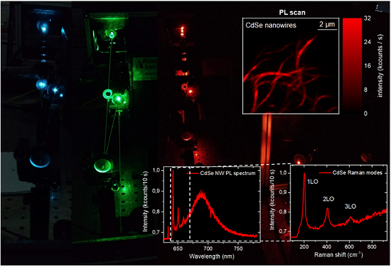
To investigate the optical properties of the semiconductor NWs, a variety of methods can be applied. We focus on confocal spectroscopy, which allows for the investigation of the photoluminescence (PL) and vibration properties of NWs in ensembles and on single-particle level. By using a variety of dedicated setups, we gain data with high temporal and spectral resolution. A PL scan of CdSe NWs with an average diameter of 9 nm, as well as a corresponding spectrum are shown in Fig. 4.
Surface-Potential Measurements
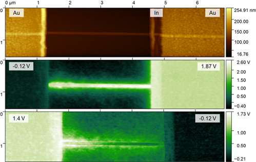
The surface potential of a sample can give insight into several different properties, e.g., the work function, surface adsorbents or the presence of stray charge carriers. In this experiment though, the most important characteristic is the potential drop along a biased nanowire, as well as the behavior of the potential at the semiconductor-metal interfaces.
For a CdS nanowire contacted by gold and indium, as it is shown in Fig. 5, it can be observed that a potential applied to the contacts drops differently along the wire, depending on the direction. This information can be used for the characterization of the contact interfaces. In this case, for example, indium creates an Ohmic contact while gold creates a Schottky contact with the nanowire. If the Schottky contact is biased in reverse, the wire charges up along with the electrode on the right, with little to no current flowing. For a forward-biased Schottky contact, electrons can flow through the nanowire and through the barrier. This is evident by a more pronounced potential drop along the nanowire.
Publications
- M. Schwarz, A. Mews, A. Dorn, Superionic Phase Transition in Individual Silver Selenide Nanowires, Nanoscale 2021, 13, 8017.
- P. Harder, A. Nielsen, A.-K. Sassnau, D. Bonatz, M. Perbandt, T. Kipp, A. Mews, Determination of the Wurtzite and Zincblende Fractions in II-VI Semiconductor Nanowires, Chemistry of Materials 2021, 33, 1061-1069.
- A. Littig, H. Lehmann, C. Klinke, T. Kipp, A. Mews, Solution-Grown Nanowire Devices for Sensitive and Fast Photodetection, ACS Applied Materials & Interfaces 2015, 7, 12184-12192.
- D. Franz, A. Reich, C. Strelow, Z. Wang, A. Kornowski, T. Kipp, A. Mews, Quantum-Confined Emission and Fluorescence Blinking of Individual Exciton Complexes in CdSe Nanowires, Nano Letters 2014, 14, 6655-6659.
- N. Reim, A. Littig, D. Behn, A. Mews, Controlled Electrodeposition of Bismuth Nanocatalysts for the Solution-Liquid-Solid Synthesis of CdSe Nanowires on Transparent Conductive Substrates, Journal of the American Chemical Society 2013, 135, 18520-18527.
- S. Schäfer, A. Reich, Z. Wang, T. Kipp, A. Mews, Charge separation in CdSe/CdTe Hetero-Nanowires Measured by Electrostatic Force Microscopy, Applied Physics Letters 2012, 100, 022110/1-022110/3.
- S. Schäfer, Z. Wang, H. U. Rammelberg, T. Kipp, A. Mews, Tip-Induced Charging of Free Standing Semiconductor Nanowires and Carbon Nanotubes, Israel Journal of Chemistry 2012, 52, 1073-1080.
- A. Myalitsin, C. Strelow, Z. Wang, Z. Li, T. Kipp, A. Mews, Diameter Scaling of the Optical Band Gap in Individual CdSe Nanowires, ACS Nano 2011, 5, 7920-7927.
- M. Böhmler, Z. Wang, A. Myalitsin, A. Mews, A. Hartschuh, Optical Imaging of CdSe Nanowires with Nanoscale Resolution, Angewandte Chemie International Edition 2011, 50, 11536-11538.
- S. Schäfer, Z.Wang, R. Zierold, T. Kipp, A.Mews, Laser-Induced Charge Separation in CdSe Nanowires, Nano Letters 2011, 11, 2672-2677.
- S. Schäfer, Z. Wang, T. Kipp, A. Mews, Fluorescence Modulation of Single CdSe Nanowires by Charge Injection through the Tip of an Atomic-Force Microscope, Physical Review Letters 2011, 107, 137403.
- Z. Wang, Z. Li, A. Kornowski, X. Ma, A. Myalitsin, A. Mews, Solution-Liquid-Solid Synthesis of Semiconductor Nanowires Using Clusters as Single-Source Precursors, Small 2011, 7, 2464-2468.
- Z. Li, X. Ma, Q. Sun, Z. Wang, J. Liu, Z. Zhu, S. Z. Qiao, S. C. Smith, G.Lu, A. Mews, Synthesis and Characterization of Colloidal Core-Shell Semiconductor Nanowires, European Journal of Inorganic Chemistry 2010, 4325-4331.
- N. Fu, Z. Li, A. Myalitsin, M. Scolari, R. T. Weitz, M. Burghard, A. Mews, One-Dimensional Heterostructures of Single-Walled Carbon Nanotubes and CdSe Nanowires, Small 2010, 6, 376-380
- Z. Li, Ö. Kurtulus, N. Fu, Z. Wang, A. Kornowski, U. Pietsch, A. Mews, Controlled Synthesis of CdSe Nanowires by Solution-Liquid-Solid Method, Advanced Functional Materials 2009, 19, 3650-3661.
- Ö. Kurtulus, Z. Li, A. Mews, U.Pietsch, X-ray Investigation of CdSe Nanowires, Physica Status Solidi A: Applications and Materials Science 2009, 206, 1752-1756.
- Z. Li, A. Kornowski, A. Myalitsin, A. Mews, Formation and Function of Bismuth Nanocatalysts for the Solution-Liquid-Solid Synthesis of CdSe Nanowires, Small 2008, 4, 1698-1702.