Nicklas Giese

Photo: Nicklas Giese
PhD student
RG Mews
Address
Office
Contact
Key aspects of activity
- Electrical characterization of charge carrier separation in a semiconductor-metal hybrid structure.
- Combined optical and atomic force microscopy in one setup.
- Electron beam and optical lithography for the generation of defined structures.
Research Topic
Nicklas Giese is investigating the charge carrier dynamics in individuel semiconductor-metal-hybrid structurs, such as metal-tipped dot-in-rod particles. The charge carriers are characterized by optical and atomic force microscopy (AFM) methods in one setup.
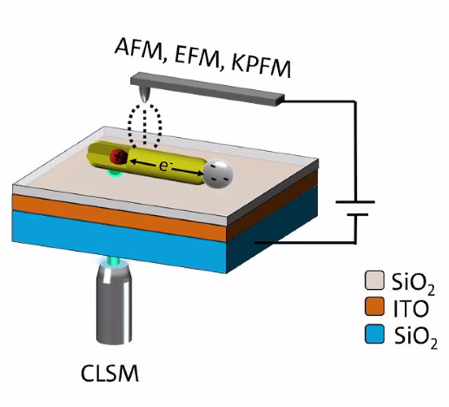
Optical excitation from below and simultaneous electrical AFM methods, such as electrostatic force microscopy (EFM) and Kelvin probe force microscopy (KPFM), are conducted for local electrical characterization. The measurements give insight into different parameters of the charge-carrier transport, e.g., the specific conductivity or the charge carrier concentration.
Optical characterization is achieved via single-particle photoluminescence (PL) spectroscopic measurements. Thereby, the incorporation of a platinium tip can be correlated to the decrease in the PL intensity of CdS giving detailed information about charge-carrier separation.

A) Schematic overview of the Setup

B) PL-Scan of a platnium marker and emitting particles

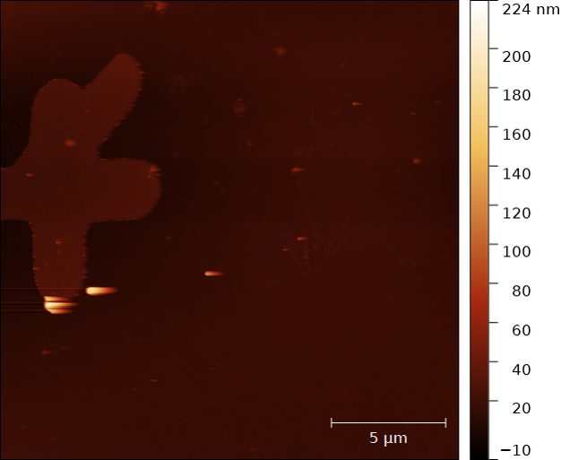
C) AFM-Image of the same section
